
SK Hynix's $26.5 Billion Nasdaq Listing Is the Biggest Foreign IPO in US History and the Money Is Headed to Korea
SK Hynix priced its Nasdaq offering at $149 per American depositary share today, raising $26.5 billion in the largest US listing by a foreign company on record. The SK Hynix biggest foreign IPO in US history surpassed Alibaba's $25 billion New York listing and Saudi Aramco's $25.6 billion Gulf debut, according to CNA and the Korea Herald. Orders came in at more than seven times the shares on offer. The proceeds are earmarked almost entirely for manufacturing facilities in South Korea, even as US policy has spent years trying to pull advanced semiconductor production closer to home.
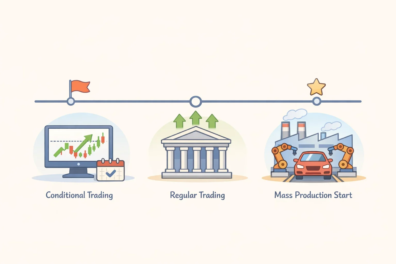
Conditional trading began today under the ticker "SKHYV." Regular trading under "SKHY" is expected to start Monday, with the offering closing Tuesday, the Korea Herald reported.
Why the largest foreign IPO in US history priced at a premium
SK Hynix issued 177.9 million American depositary shares, each representing one-tenth of a common share traded in Seoul, at $149 apiece. That structure lets foreign companies trade on US exchanges without a full domestic relisting, CNA explained. The new shares equal about 2.5% of the existing share count, so dilution is minimal for what is, by any measure, an enormous capital raise, the Korea Herald noted.
Large equity offerings are typically priced at a discount to draw buyers. SK Hynix priced at a roughly 2.9% premium to its Seoul close the prior day and still saw seven-times oversubscription which the company said made it the first US IPO of its kind priced above the prevailing market price, according to the Korea Herald. That combination is unusual enough to warrant some explanation.
Dilin Wu, research strategist at Pepperstone, told AFP the pricing confirms "the AI memory cycle is real, the earnings are real," and called the listing "a huge development that should broaden the capital base for the memory sector," per CNA. SK Hynix is a primary supplier of advanced memory chips to Nvidia, and its profits have surged alongside the global buildout of AI data centers.
The Nasdaq listing is also expected to help SK Hynix close a valuation gap with Micron by making its shares more accessible to overseas investors, the Korea Herald reported. SK Hynix's market cap crossed $1 trillion on Seoul's Kospi in May, joining a club of roughly a dozen companies globally, nearly all American, per CNA. SK Group Chairman Chey Tae-won said earlier this year that the ADR listing would give the company "greater exposure to US and global shareholders" and help make it "a more global company," the Korea Herald reported.
The offering was led by BofA Securities, Citigroup Global Markets, Goldman Sachs (Asia), and JPMorgan Securities.
Where the $26.5 billion is actually going
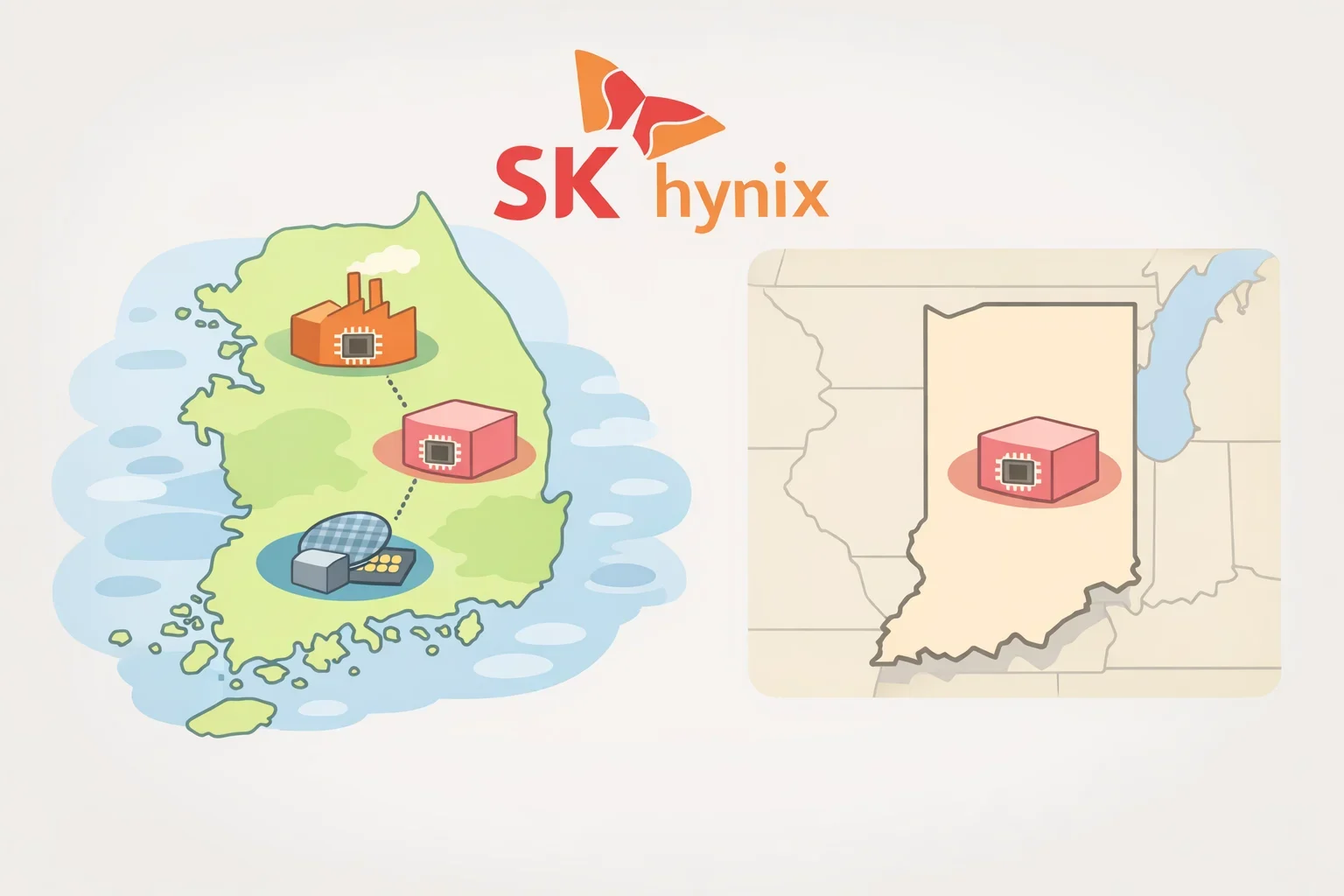
The use-of-proceeds disclosure leaves little ambiguity. Per a regulatory filing cited by the Korea Herald, the funds will go toward construction of the first fabrication plant at the Yongin semiconductor cluster near Seoul, the P&T7 advanced packaging facility in Cheongju, and manufacturing equipment purchases. The company has separately earmarked 11.9 trillion won for extreme ultraviolet lithography tools, to be installed by end of next year.
SK Hynix is also part of an 800 trillion won public-private initiative, alongside Samsung, to develop a new chip hub in southwest South Korea, CNA reported. Counterpoint Research analyst MS Hwang told AFP the company wants to extend its HBM technology lead into a volume lead as well, adding that "funds from its US listing can support such a goal." Counterpoint has forecast operating margins of 75% to 80% for Samsung, SK Hynix, and Micron in Q2, the Korea Herald noted, which gives all three strong reasons to expand capacity aggressively.
SK Hynix does have a US footprint, though it is narrower than the word "fab" implies. The Department of Commerce awarded the company up to $458 million in CHIPS Act direct funding to build an HBM advanced packaging and R&D facility in West Lafayette, Indiana, backing a total investment of approximately $3.87 billion at a site adjacent to Purdue University, according to NIST. Mass production there is expected to begin in the second half of 2028, with the facility supporting roughly 1,000 jobs.
That site is an advanced packaging and R&D facility, not a front-end wafer fab. Packaging is the final stage of chip assembly. Front-end fabrication, the process of printing circuits onto silicon wafers, is a separate and considerably more capital-intensive undertaking, and it is front-end capacity that SK Hynix is building in Yongin with the proceeds from this week's listing.
The economics of US fab expansion don't easily cooperate
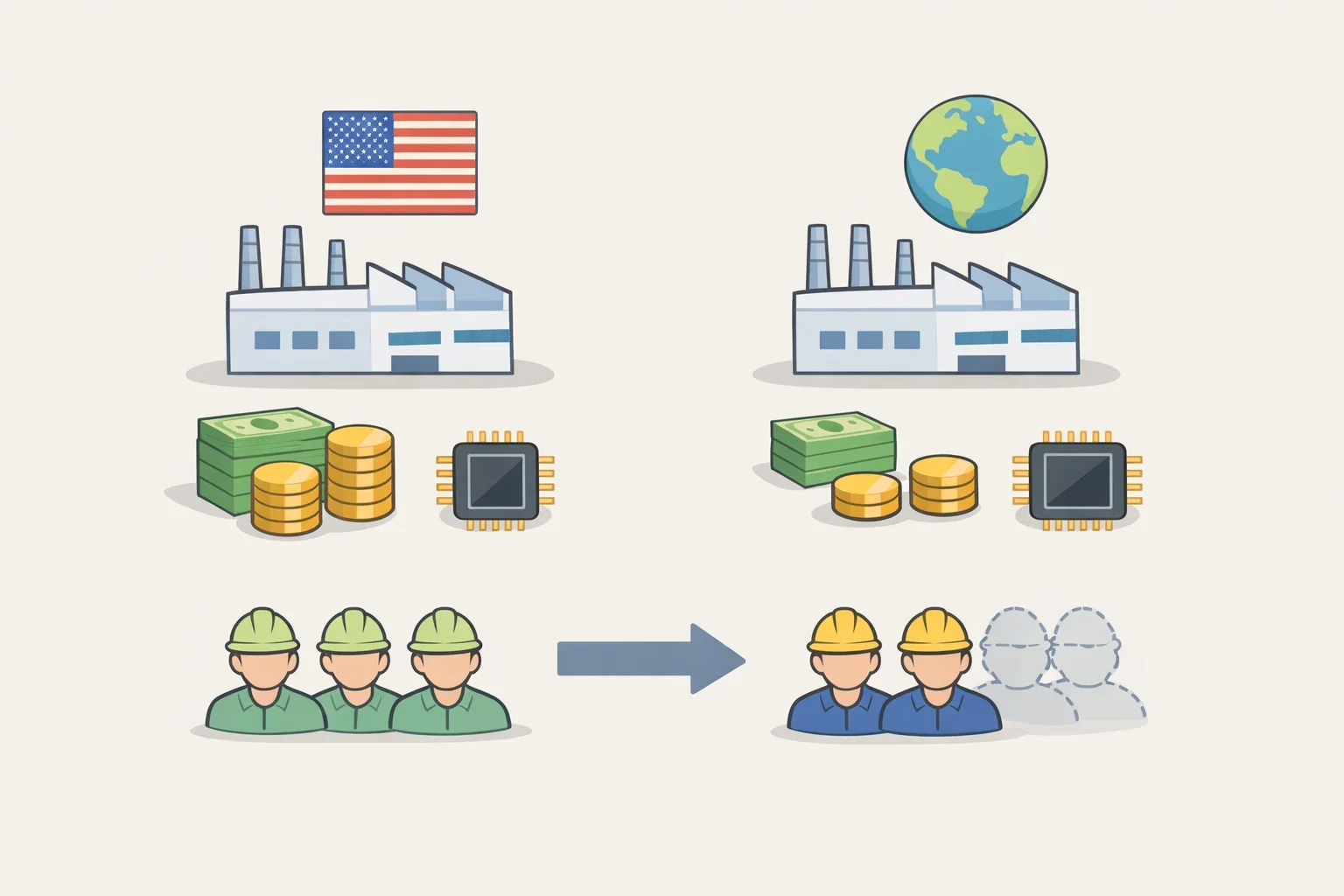
Building a new semiconductor fab in the United States costs approximately 20% more than an equivalent facility in Taiwan or South Korea, with operating costs adding a further structural disadvantage, according to a Yale Journal of International Affairs analysis published last year. The CHIPS Act has attracted nearly $450 billion in private capital and spurred more than 90 semiconductor projects across 22 states, with US fabrication capacity projected to grow 203% by 2032. The workforce to staff those facilities, though, is not yet there. The industry will need 115,000 additional skilled workers by 2030, including 67,000 in manufacturing roles alone, the same Yale Journal analysis found.
The scale gap is stark. The CHIPS and Science Act appropriated $52.7 billion for fiscal years 2022 through 2027, per Congress.gov. US semiconductor firms spent roughly $109.6 billion on capital expenditures and R&D in 2022 alone, the Yale Journal reported, which puts the federal outlay in perspective. Prior CHIPS recipients, including TSMC, delayed US manufacturing timelines by roughly two years while negotiating over subsidy terms and other conditions, suggesting that even well-capitalized companies treat the cost differential as a genuine constraint, not an accounting footnote.
For memory specifically, front-end DRAM fabrication requires dense supplier ecosystems and years of ramp time to reach competitive yields. The Indiana facility addresses a real strategic gap HBM packaging is a critical component of the GPUs used to train AI systems, per NIST. But it is a different undertaking than replicating the Yongin cluster on US soil.
What comes next
SK Hynix's record US listing is, at one level, a clean financing story: the dominant player in AI memory raises capital at favorable terms to extend its manufacturing lead. US investors funded that at premium valuations, and the seven-times oversubscription removed any doubt about demand.
The CHIPS Act committed $458 million to anchor SK Hynix's Indiana presence. Whether that foothold expands into something larger, or the West Lafayette site remains a packaging and R&D enclave while front-end production stays concentrated in Korea, depends on economics and policy continuity that remain unsettled.
What is settled: conditional trading is live today under "SKHYV," regular trading under "SKHY" begins Monday, and the proceeds are committed to facilities in Yongin, Cheongju, and the broader Korean semiconductor buildout. The Indiana mass production line comes online in 2028. That is the timeline US policymakers are working with.
