

QuantumDiamonds Funding Round: TUM Spinout Raises €91M for Chip Inspection
Seven of the world's ten largest semiconductor companies have been sending proprietary chips to a three-year-old Munich startup for testing. That is not a sales pipeline. It is an unusually concrete vote of confidence from an industry that does not share hardware with companies it does not take seriously.
The QuantumDiamonds funding round totals €91 million, though only €15 million of that has been disclosed as equity. That equity round was led by Berlin-based deep-tech investor World Fund and joined by existing backers Bayern Kapital, Creator Fund, Earlybird, First Momentum, IQ Capital, Onsight Ventures, and UnternehmerTUM, TechCrunch reported this week. The company said the package also includes EU backing, though the exact composition of that support has not been disclosed. No valuation was released.
The financing is the news. The harder question is what QuantumDiamonds needs to do with it. The company has built a chip inspection tool that can see inside a wafer stack in ways that conventional metrology cannot. It currently takes about 10 minutes per measurement. For the technology to move from specialist diagnostic instrument to production-line tool, that needs to drop below one minute. That gap is the story.
What the tool actually does
QuantumDiamonds was founded in November 2022 as a spinout from the Technical University of Munich. The company initially pursued applications in biology, chemistry, and semiconductor manufacturing, per EE Times, but has since focused almost entirely on semiconductors, where the commercial urgency is sharpest.
The core problem it targets is a genuine blind spot in current fab practice. Standard metrology tools can image the top layer of a chip, but not what lies beneath it. In modern 3D chip architectures, defects buried in bonded layers, through-silicon vias, or deep interconnects go undetected until they cause failures, often not until after packaging, when catching them is far more expensive, EE Times reported in late 2024. "Using current methods for metrology, it's really hard to do imaging in different layers," CTO and co-founder Fleming Bruckmaieri told EE Times.
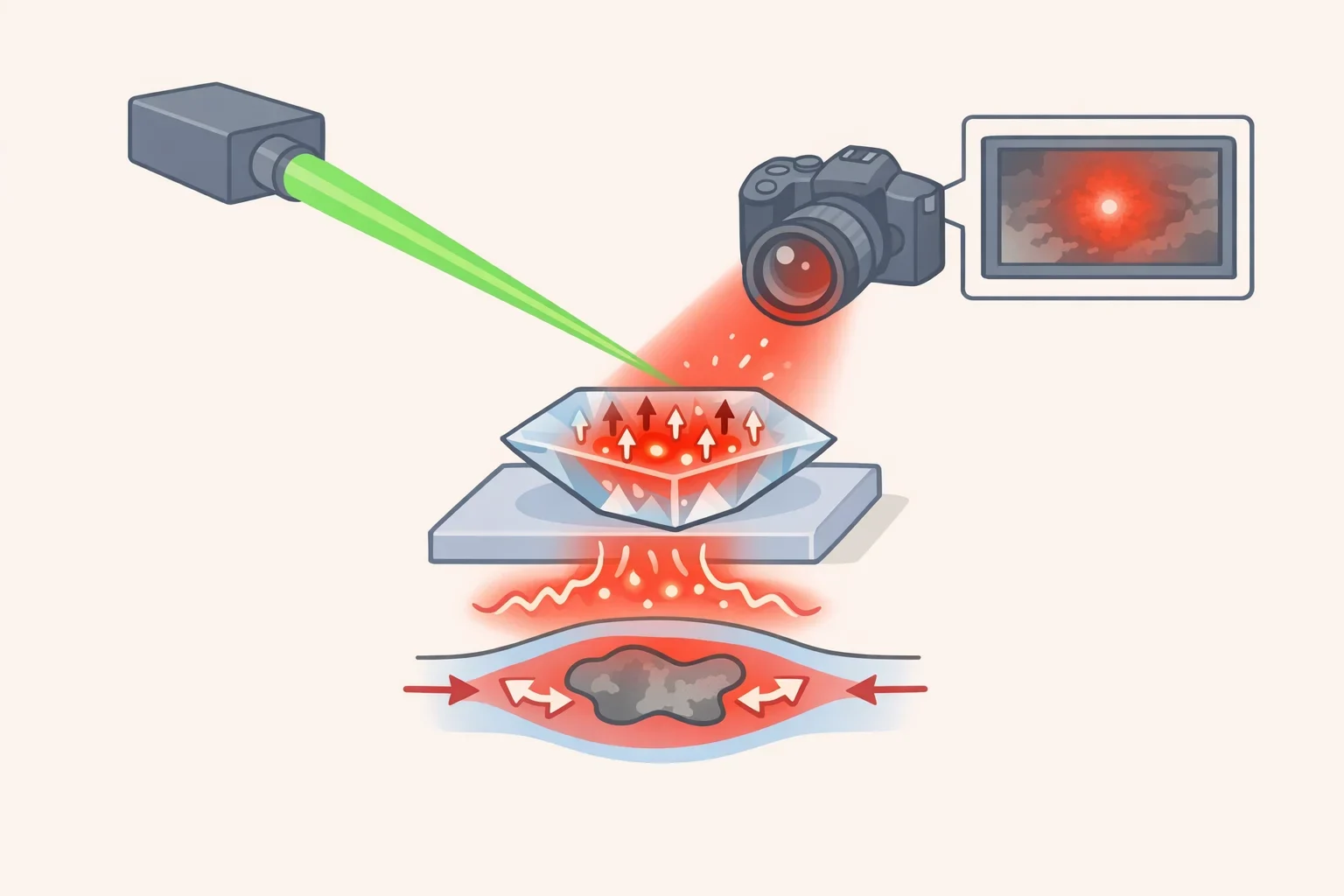
The sensor works by directing a green laser at a synthetic diamond through a microscope objective. That excites quantum spins in the diamond, causing it to emit red light captured by a camera. The resulting magnetic field map highlights current-density anomalies. "In a functioning chip, the current distribution is homogeneous, whereas in a failing chip, peaks in the current density indicate opens, shorts or material defects that require investigation," CEO Kevin Berghoff explained to EE Times.
The company claims the tool can probe a wafer structure to a depth of 100 microns, "which is pretty deep," in the words of one independent industry observer quoted by EE Times, and can resolve features down to the nanometer scale under ideal conditions. Those figures come from the company itself; no independent benchmarking against incumbent tools has been published.
One point worth being clear about: this is currently a failure-analysis tool. It diagnoses chips that have already been flagged as suspect. It is not running inline on a production floor, screening every wafer in real time. The distinction matters for how the customer engagement and the funding should be read.
Early traction and what it does and does not prove

The customer engagement is notable. Seven of the ten largest semiconductor companies have sent chips to QuantumDiamonds' Munich labs for testing, Berghoff told EE Times. Companies at that scale do not casually hand over proprietary hardware. The fact that they did, when the company was under two years old at the time, suggests the technology cleared some internal threshold of credibility.
The deployment roadmap was also concrete, at least as reported. The company expected to deliver its first device to Germany's Fraunhofer Institute by December 2024, with testing labs in Taiwan and the United States to follow in early 2025, EE Times reported. Whether those installations went ahead on schedule has not been independently confirmed. What those early deployments showed is more informative than any funding announcement, and that data is not yet public.
McKinsey's 2025 quantum technology monitor noted the launch of QuantumDiamonds' diamond-based microscopy tool for semiconductor failure analysis, providing external corroboration that the company had shipped a real product, even if detailed performance data remains unavailable.
In deep-tech hardware, that combination, top-tier customers sharing proprietary chips, an institutional partner willing to take a first device, an independent analyst noting a product launch, represents meaningful progress. It does not, by itself, prove a path to production adoption.
What the QuantumDiamonds funding round needs to achieve
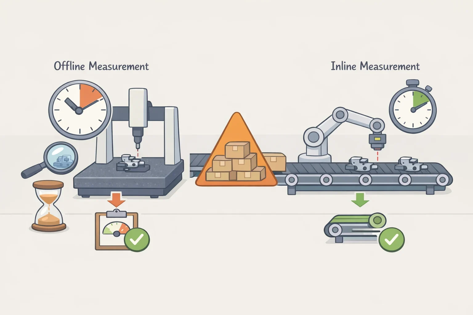
The specific obstacle standing between QuantumDiamonds' current tool and a production fab floor is measurement speed. Inline metrology has non-negotiable requirements: the process must be non-destructive and must not take components offline, EE Times noted. Measurements also need to complete in roughly one minute to avoid creating throughput bottlenecks on the production line.
QuantumDiamonds currently takes about 10 minutes per measurement, depending on chip size and component density, EE Times reported in late 2024. That makes it a capable offline diagnostic tool. It makes it roughly an order of magnitude too slow for inline deployment.
The sensing physics is not the limiting factor. "The biggest bottleneck is the volume of data that has to be analyzed," Berghoff told EE Times. The sensing mechanism works; the data pipeline needs to catch up. The company's target is to bring measurement time below one minute, which frames a significant portion of this capital raise as a data engineering and productization investment, not fundamental research.
That framing also explains the financing structure. The package combines EU backing with venture equity from investors including World Fund and IQ Capital, TechCrunch reported this week. European deep-tech hardware companies at this stage, working technology, genuine customer interest, long development cycles ahead, often require capital structures that blend public and private sources. Pure venture timelines and pure grant bureaucracies each create their own constraints. A hybrid package sidesteps the worst of both.
Whether it provides enough runway depends on how quickly the team can close the gap between 10 minutes and one. Hit that target, and a niche failure-analysis tool becomes a credible candidate for inline production metrology at some of the largest chipmakers on earth. Miss it, and the addressable market stays smaller and the competitive position more fragile.
The physics is solid enough that the industry is paying attention with something more valuable than compliments. The engineering is where this gets decided.
